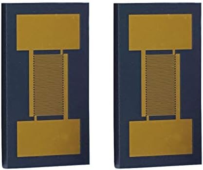


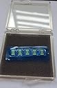
2 Pieces Interdigitated Electrode Array capacitance Monocrystalline Silicon Chip Gold Electrode (Big)
Buy anything from 5,000+ international stores. One checkout price. No surprise fees. Join 2M+ shoppers on Desertcart.
Desertcart purchases this item on your behalf and handles shipping, customs, and support to Belgium.
Description
- 1. This interdigital electrode is widely used in chemical, physical and medical sensors, with reliable performance and stable quality!
- 2. Electrode substrate is monocrystalline silicon with 300nm thickness of SiO2 on the surface of the silicon wafer.
- 3. The suitable temperature for using is from - 100 degrees Celsius to +400 degrees Celsius.
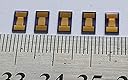
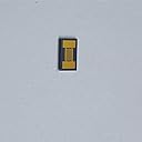
- 4. overall size: 4mm*7mm.
- 5. Electrode resistance is more than 100T ohm (room temperature, humidity 64%)
Size:Big 1. overall size: 4mm*7mm. 2. Line Width: 30um, line space: 20um. 3. Electrode substrate is monocrystalline silicon with 300nm thickness of SiO2 on the surface of the silicon wafer. 4. Conductor layer structure: Cr/Au, the thickness are10nm and 100nm respectively. 5. The suitable temperature for using is from - 100 degrees Celsius to +400 degrees Celsius. 6. Electrode resistance is more than 100T ohm (room temperature, humidity 64%).
Common Questions
Trustpilot